Centre for Applied Research
Technology Campus Teisnach Sensor Technology I 4.0
Academic Staff
TCTS O 17
09923/80108-506
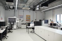
Material and surface analysis
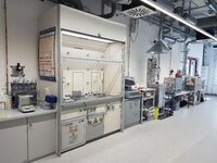
TC Teisnach
Material and layering technology